saifysyed
Pakistan

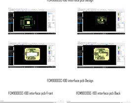
I am going to make interface pcb for wifi chip, FCN9000SC-100.
Please refer to 3 docs.
1. design guide of FC9000.pdf
2. wifiboard-RCB9000SC-100.pptx
3. sketch_schematic_n_pcb.jpg
And refer to http://static6.arrow.com/aropdfconversion/997dc941a7755fbe455ee11d374498ce9fc9ddf/fcm9000s_series_datasheet_ver1.0_180123_l.pdf
Pcb should be full patterned by GND and connector J3 is female header put on the opposite side of wifiboard. and J4 is not a connector but TP.
Please see pull up and down and by pass capacitors.
I can not edit the submission file type.
Please be sure that submission file is gerber files of PCB and image files of pcb.

Post Your Contest Quick and easy

Get Tons of Entries From around the world

Award the best entry Download the files - Easy!